Power Diode – Construction, Types & Its Applications
Power Diode – Construction, Types & Its Applications
The diode is a simple semiconductor device that includes two
layers, two terminals & a single junction. The junction of normal diodes
can be formed through semiconductors like p-type and n-type. The terminal at
the p-type is known as the anode whereas the terminal at the n-type is known as
the cathode. There are different kinds of diodes available in the
market. Each type has its application. This article discusses an overview of
the power diode. Ideally, a diode must have no reverse recovery time. But, the
deigning cost of such a diode may change. In various applications, the reverse
recovery time effect is not important so low-cost diodes can also be used.


Definition: A power diode or high-power diode is one of the power semiconductor devices that have two terminals (cathode and anode) similar to the normal PN junction diode but exhibit higher power handling capability. These are designed to handle several kiloamps of current in forward biased condition with negligible power loss and must block several kilovolts under reverse-biased state.
More simply, we can say that power diodes are devices that are designed to carry a large amount of current at high voltage. Power semiconductor devices mainly find their use in power electronic circuits.
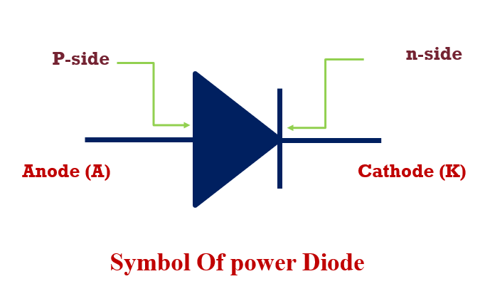
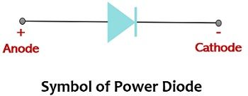
Symbolically a power diode is represented as:
Before elaborating more about power diodes, it is important to recall-
A normal diode is a low-power diode that has a PN junction and is also known as a signal diode. We have already discussed in our previous content on diodes that a diode offers unidirectional flow of current. It is a combination of p and n-type semiconductor materials that conduct when forward biased and block the flow of current when reverse biased.
A power diode also has a PN junction that permits the flow of current in a single direction only. But it differs from that of a low-power diode in terms of its construction and the features offered. From features here we mean the enhanced level of voltage, current, and power ratings provided by high power diodes. Also, unlike signal diodes, these operate at lower switching speeds.
Basics of PN junction
The fundamental entity that is responsible for the operation of various power semiconductor devices is a p-n junction. Even in signal diodes, we have seen that a p-n junction is formed by physical contact between p and n-type semiconductor materials.
We are already familiar with the basics that p-type has majority holes and minority electrons while n-type has majority electrons and minority holes. However, to form power diodes variation in concentration of p and n types of materials is required. A p-type material can be denoted as p+, p, and p-, and n-type can be designated as n+, n, and n– according to variation in doping concentration.
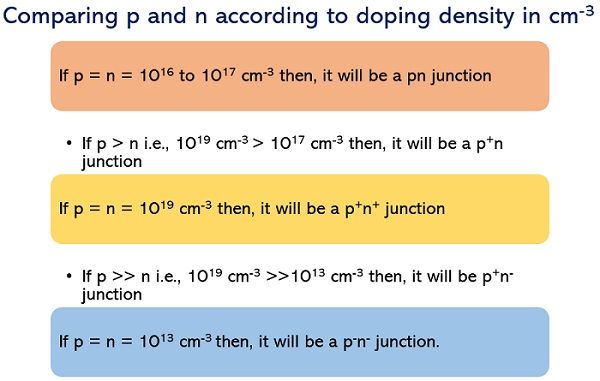
Thus, in general, we can conclude p+ as a highly doped p region and n– as a lightly doped n region.
Need for Power Diodes?
Basically, the signal diodes are used in low-power rectification circuits. However, in all such applications where large forward-biased current and high reverse-biased blocking voltage are needed, the small-signal diodes do not perform well. This is so because signal diodes are not constructionally built to handle such a large current so in case a large current is provided then they will be overheated resulting in destroying the device.
Thus, to overcome the drawbacks of signal diodes, power diodes came into existence.
Now, the question arises how does it do so?
A power diode offers a comparatively larger p-n junction region than a signal diode. Thus, it offers a high forward current capability that ranges several hundred amps and a large value of blocking the reverse voltage i.e., up to several thousand volts.
Construction
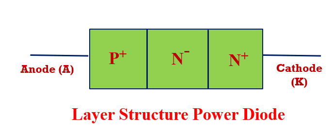
The construction of this diode includes three layers like the P+ layer, n– layer and n+ layer. Here the top layer is the P+ layer, it is heavily doped. The middle layer is n– layer, it is lightly doped and the last layer is n+ layer, and it is heavily doped.
The constructional structure of power diodes is shown below:

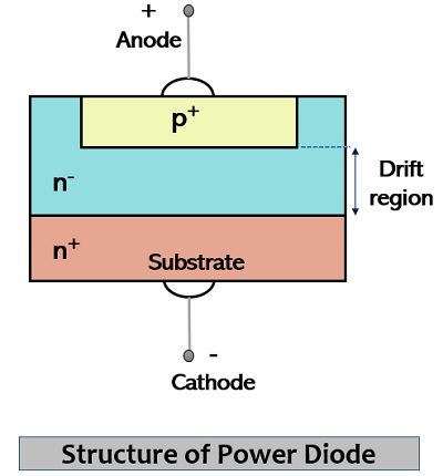

An n+ heavily doped substrate is considered over which epitaxially an n– layer is grown, moreover, diffusion of p+ layer takes place over the n– region. This p+ region forms the anode connection while the n+ substrate forms the cathode connection.
Here p+ layer acts as an anode, the thickness of this layer is 10 μm & the level of doping is 1019 cm-3. The n+ layer acts as a cathode, the thickness of this layer is 250-300 μm & the level of doping is 1019 cm-3. The n- layer acts as a middle layer/drift layer, the thickness of this layer mainly depends on the breakdown voltage & the level of doping is 1014 cm-3. Once this layer width increases then breakdown voltage will be increased.
Working Principle of Power Diode
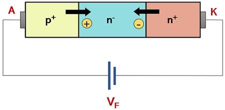
The working principle of this diode is similar to the normal PN junction diode. When the voltage of the anode terminal is high than the voltage of the cathode terminal, the diode conducts. The range of forwarding voltage drop in this diode is very small approximately 0.5V – 1.2V. In this mode, the diode works as a forward characteristic.
If the voltage of the cathode is high than the voltage of anode, the diode performs as blocking mode. In this mode, the diode performs like the reverse characteristic.
Consider the forward biased condition of a power diode shown below, where the positive terminal of the battery is connected to the anode and the negative terminal forms a connection with the cathode.
Now, consider the reverse biased condition, where the negative terminal of the battery forms a connection with the anode and the positive terminal is connected to the cathode.
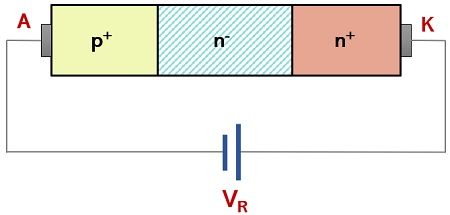
But it is to be noted here that a sudden change in polarity of applied potential will not immediately stop the flow of current. Moreover, the minority charges stored in the junction will lead to the flow of small leakage current (of order 100 mA) through the diode in opposite direction. This reverse current shows dependency on variation in junction temperature.
Once the applied potential becomes equal to the breakdown voltage, then impact ionization will take place.
Types of Power Diode
The classification of these diodes can be done based on the reverse recovery time, the process of manufacturing & the depletion region penetration in reversed bias condition.
The power diodes depending on the reverse recovery time as well as the process of manufacturing are classified into three type
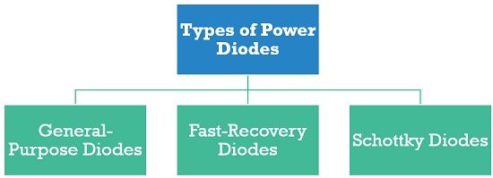
- General Purpose Diodes: These diodes have huge reverse recovery time around 25μs (25 microseconds); therefore they are applicable in low frequency (up to 1 kHz) & low-speed operations (up to 1- kHz). Its current rating lies between 1 A to several thousand amperes and its voltage rating lies between 50 V to 5 KV.
- Fast Recovery Diodes: These diodes have quick recovery act due to their very small reverse recovery time less than 5μs (5 microseconds), used in high-speed switching applications Mainly used in electrical power conversion systems. Its current rating lies between 1 A to several thousand amperes and its voltage rating lies between 50 V to 3 KV.
- Schottky Diodes: In these diodes instead of p-n junction, metal-semiconductor junction is formed where generally aluminium is preferred for metal and silicon for semiconductor. Its current rating lies between 1 A to 300 A while the reverse voltage rating is about 100 V.
The power diodes can be classified into the following categories, summarized in the table below, as per their properties:
Type | Voltage ratings (VRRM) | Current ratings (IF) | Reverse recovery time (trr) | Applications | Remarks |
General Purpose Diodes | 50-5000 V | 1A to several thousand Amps | ~25µs | UPS, battery chargers, welding, traction, etc. | – |
Fast Recovery Diode | 50-3000 V | 1A to several thousand Amps | <5µs | SMPS, commutation circuits, choppers, induction heating | Doping is done using platinum or gold |
Schottky Diodes | Up to 100V | 1-300 A | ~ns | Very high frequency switching power supplies and instrumentation | Metal-semiconductor junction, usually Al-Si(n-type), majority carrier device, hence very low turn off time |
The power diodes depending on the penetration of the depletion region are reversed biased condition are classified into two types such as
- Punch through Diodes
- Non-Punch through Diodes
Punch through Diodes
Diode, where the width of the depletion region at the breakdown enters into the n+ layer, is known as a punch-through diode.
Non-Punch through Diodes
A diode where the width of a depletion region at the breakdown doesn’t go through into the adjacent n+ layer is usually called non-punch-through diodes.
In this mode, the drift region’s width is extra than the highest width of the depletion region, therefore the depletion region cannot enter into the adjacent n + layer.
Classification Of Diode
Majorly there are two classifications in diodes.
- Power Diode
- Signal Diode
For power diodes, its an advantage that they handle high power but…. at low frequency. Ex. SCR’s
For signal diodes, they operate in very high frequencies (MHz, GHz ranges) but have very low power handing capacity. Ex: MOSFET’s
Finally to obtain both at an average level, IGBT’s came in to existence which have a comparably speed and power handling capacity.
So here is the relation in diodes…. Power inversely proportional to frequency . i.e., if u want to operate at high power, forget about frequency.
How to Select?
The selection of power diode can be done based on the IF (forward current) & VRRM (the peak inverse) voltage.
These diodes are protected by using snubber circuits from the spikes of overvoltage. This may occur while doing the process of reverse recovery. A snubber circuit used for power diode mainly includes a resistor & a capacitor that is connected in parallel with the diode.
V-I Characteristics of Power Diodes
The V-I characteristics of a power diode are shown below. Once the forward voltage increases then the forward current will be increased linearly.
An extremely less amount of current leakage will supply in the reverse bias condition. This current is independent of the applied reverse voltage.
The leakage current mainly supplies because of the minority charge carriers in the diode. As the reverse voltage gets the reverse breakdown voltage, then the breakdown of an avalanche will occur. When the reverse breakdown arises, the reverse current will also be raised drastically with less increase in reverse voltage. The reverse current can be controlled by an external circuit.
The figure below shows the v-i characteristics of a power diode which is almost similar to that of a signal diode.
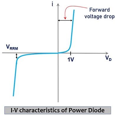


In signal diodes for forward, a biased region the current increases exponentially however in power diodes high forward current leads to high ohmic drop which dominates the exponential growth and the curve increases almost linearly.
The maximum reverse voltage that the diode can withstand is depicted by VRRM, i.e. peak reverse repetitive voltage.
Above this voltage, the reverse current becomes very high abruptly and as the diode is not designed to dissipate such a high amount of heat, it may get destroyed. This voltage may also be called peak inverse voltage (PIV).
Reverse Recovery Characteristics of Power Diodes

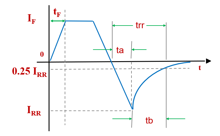
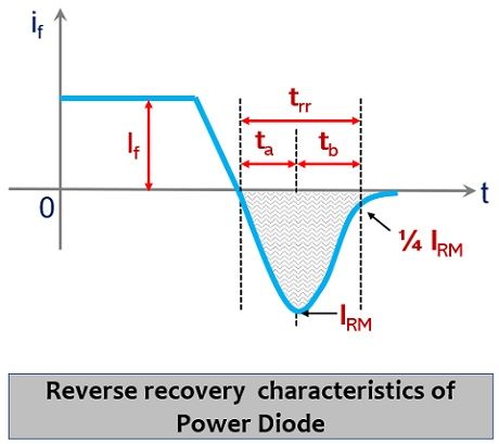
The figure depicts the reverse recovery characteristic of a power diode. Whenever the diode is switched off the current decays from IF to zero and further continues in reverse direction owing to the charges stored in the space charge region and the semiconductor region.
he AC diode is characterized by the Forward recovery time (tF) and reverse recovery time (trr) .
Forward recovery time (tF): Forward recovery time is the time required by a diode to start conduction is called forward recovery time. In other words time taken by a diode to switch from off state to on state is called Forward recovery time (tF).
Reverse recovery time (trr) : After the forward diode current decays to zero, the continue to conduct in the reverse direction because of the presence of the stored charges in the two layers . The reverse flow for a time called reverse recovery time (trr). The diode retain its blocking capability until reverse recovery current decays to zero.
The reverse recovery time is define as the time between the instance forward diode current become zero and the instant reverse recovery current decays to 25% of its reverse peak value Irm.
The reverse recovery time is the combination of two segment of time ta and tb i.e. trr = ta + tb where time ta is the time between zero crossing of forward current and peak reverse current Irm. During the time ta, charged stored in depletion region is removed. Time tb is measured from the instant of Irm to the instant where 0.25 Irm is reached. During tb carge two semiconductor is removed.
The ratio of ta/tb is called softness factor or S-factor. The diode with softness equal to one is called soft recovery diode and diode with softness factor less than one is called snappy recovery diode or fast recovery diode.
This reverse current attains a peak IRR and again starts approaching zero value and finally, the diode is off after time trr.
This time is defined as reverse recovery time and is defined as the time between the instant forward current reaches zero and the instant the reverse current decays to 25% of IRR. After this time the diode is said to attain its reverse blocking capability.
From the figure above, we see that
ta → time when charge from depletion region is removed
tb → time when charge from semiconductor region is removed
Also from the figure, we can say that
Where,  is the rate of change of reverse current.
The area bounded by the triangular region in the above figure represents the total charge stored or reverse recovery charge, QR. Hence we can write
Now, for , putting in eq.1 and combining with eq.2, we get
Putting eq.3 in eq.1 for, we get
From eq. 3 and 4 we can see that trr and IRR depend on QR which in turn depends upon the initial forward diode current IF.
Another interesting parameter is defined for power diodes from its turn-off characteristics known as Softness Factor (S-factor) defined as the ratio of times tb and ta.
Hence,
If a diode has S-factor equals to unity it is known as a soft-recovery diode and for S-factor less that unity it is known as fast or snappy-recovery diodes.
S-factor indirectly indicates the voltage transient that occurs upon the turn off of the diode. Low S-factor implies high transient overvoltage while high S-factor implies low oscillatory reverse voltage.
The total power loss during turn off is the product of diode current and voltage during trr. Most of the power loss occurs during tb.
In a typical datasheet of power diodes the most important parameters given are IF avg, IF RMS, VRRM, I2t rating, junction temp TJ, trr, S-factor, IRR. Apart from these many other parameters and graphs are also provided.
Advantages and Disadvantages of Power Diode
The advantages and disadvantages of power diode include the following.
- The PN-junction region of this diode is large & can supply huge current, however, the capacitance of this junction can also be large, which works at a lower frequency & it is generally used for rectification only.
- It will resolve AC at high current and a high voltage.
- The main disadvantage is its size & probably needs to be fixed to a heat sink while conducting a high current.
- It needs specialized hardware for installing and insulating from the metal frames which are available in the surrounding.
Applications
Due to the characteristics of power diodes, these are mainly used as freewheeling diodes, in ac to dc and dc to ac conversion systems, rectification, battery charging, etc. Along with these, power diodes are also used in electroplating, UPS, choppers, SMPS, and induction heating as well. The applications of power diode include the following.
- This diode provides uncontrolled power rectification
- It is used in different applications like DC power supplies, for charging the battery, inverters and AC rectifiers.
- These are used like snubber networks and free-wheeling diodes due to their characteristics like voltage & high-current.
- These diodes are used as feedback, freewheeling diodes, and high-voltage rectifier.
- In reverse breakdown condition, when the current and voltage of this diode are huge, the power dissipation can be high so the device can be destroyed.
Q. What is the function of a power diode?
Answer: It is a type of crystalline semiconductor, used to change AC to DC and this process is called rectification.
Answer: These diodes are used where high voltages & larger currents are involved.
Answer: They are fast recovery, Schottky & general-purpose diodes.
Answer: Power diode is applicable for where high current & voltage are used like inverter whereas normal diode is applicable for small-signal applications.
Answer: A power diode is a type of diode that is commonly used in power electronics circuits. The power diode is a simple semiconductor device that includes three layers, two terminals, a single junction & conducts current in one direction. In order to increase the power handling capacity, we use power diode by small changes in the structure of simple p- n junction diode.
Answer: For power diodes, it’s an advantage that they handle high power but…. at low frequency. Ex. SCRs for signal diodes, they operate in very high frequencies (MHz, GHz ranges) but have very low power handing capacity. Ex: MOSFET’s
Answer: Forward recovery time is the time required by a diode to start conduction is called forward recovery time. In other words, time taken by a diode to switch from off state to on state is called Forward recovery time (tF).
Answer: The reverse recovery time is defined as the time between the instance forward diode current become zero and the instant reverse recovery current decays to 25% of its reverse peak value Irm.
Q. What is impact ionization?
Answer: The reverse applied voltage excites the electric field due to which the electrons will get accelerated. After gaining sufficient kinetic energy, the moving electrons may be able to liberate more electrons from the covalent bonds of silicon atoms. This cumulative process generates a large number of free electrons due to which large reverse current flows through the device. This large reverse current considerably increases the power dissipation hence may lead to destroying the diode. Thus, it is said that the operation of the device in the reverse breakdown region must be avoided.
Answer: The reverse recovery time is the combination of two segment of time ta and tb i.e. trr = ta + tb where time ta is the time between zero crossing of forward current and peak reverse current Irm. During the time ta, charged stored in depletion region is removed. Time tb is measured from the instant of Irm to the instant where 0.25 Irm is reached. During tb carge two semiconductor is removed. The ratio of ta/tb is called softness factor or S-factor. The diode with softness equal to one is called soft recovery diode and diode with softness factor less than one is called snappy recovery diode or fast recovery diode.
Comments
Post a Comment